
Semiconductor Device Program
Research
Low Power Design of Analog High-Frequency Integrated Circuits
In today’s society, semiconductor integrated circuits, which are essential for modern living, demand continuous
performance improvement. However, for mobile applications and in pursuit of a low-carbon society, there is also
a need to balance conflicting characteristics such as miniaturization and reduced power consumption. This
research primarily focuses on communication systems, which are often performance bottlenecks, and aims to
develop circuit design techniques that reconcile these opposing characteristics. From the initial design phase
to prototyping and evaluation, our research contributes to enhancing the performance of semiconductor devices,
meeting the high demand both domestically and internationally.
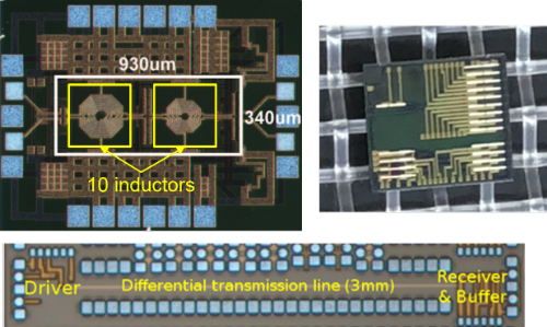
Semiconductor Integrated Circuit Design Examples:
[Top Left] High-Efficiency Driver for Optical Communication (180nm CMOS)
[Top Right] InP Optical Integrated Circuit for Terahertz Wireless Communication
[Bottom] Low-Power On-Chip Communication System (90nm CMOS)
Noise Reduction in Image Sensors
In Image Sensors used for video recording and machine recognition, noise can degrade image quality and cause
errors in automated recognition. To understand the mechanism behind noise generation and to mitigate it, we
combine experimental evaluation and computer simulations to study the behavior of impurities and defects in the
semiconductor, which are the root causes of noise. Additionally, we work to establish noise reduction techniques
that contribute to the enhancement of image sensor performance.
Web site (Semiconductor-Process Evaluation Lab.,Suzuki Research Group)
Introduction of cleanroom (Youtube)
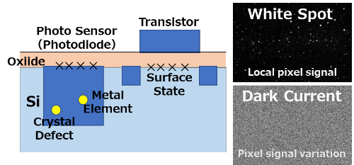
Schematic Diagram of an Image Sensor (Left) and Examples of White Spot and Dark Current Images (Right)
Energy Storage and Conversion Materials
Dielectrics possess the ability to instantaneously store and release electrical energy, making them
indispensable for the high-speed and stable operation of semiconductor devices. Moreover, some dielectrics have
the capacity to convert stress or light into electrical energy through energy conversion processes. These
functionalities are intricately linked to the electronic states, crystal structures, lattice defects, and domain
structures of materials. Through a collaborative approach that combines experimental research and theoretical
calculations, we focus on understanding the behavior of atoms and electrons to design novel dielectric
materials. We synthesize ceramics, thin films, and single crystals, contributing to the development of new
materials that will advance next-generation semiconductor devices and energy conversion devices.
Web site (Energy Material/Functional
Materials Lab.)

Hierarchical Structure of Barium Titanate Ferroelectric Ceramic, from Micrometer to Atomic Scales. Trace
amounts of impurity elements (Fe) and oxygen vacancies (VO) also have a significant impact on its
properties.
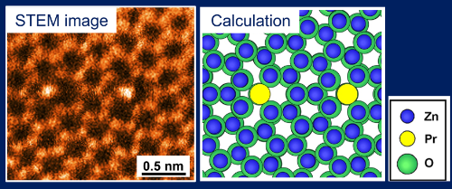
Examining the Source of Functionality at the Nano and Atomic Scales
In our research group, we aim to uncover the mechanisms behind the functioning and malfunctioning of
semiconductor devices. Our goal is to contribute to the development of new devices and the enhancement of their
performance based on this understanding. To conduct our research, we utilize tools such as Scanning Transmission
Electron Microscopy (STEM), which allows us to observe materials at the atomic and electron scale, as well as
first-principles calculations, which enable simulations at the atomic and electron scale.
For example, in the illustration provided, we elucidated the atomic-level structure of grain boundaries in zinc
oxide (ZnO), a known oxide semiconductor. These grain boundaries were found to be hindering the flow of current.
Our research aims to uncover such detailed structures and mechanisms that influence semiconductor behavior,
paving the way for advancements in semiconductor technology.
Web site (Functional Nanostructures
Laboratory)
Next-Generation Compound Semiconductor Devices
The development of next-generation semiconductor materials with superior properties compared to conventional
semiconductor materials is progressing. However, these materials have only been practically applied in specific
device structures. This is primarily because the surface and interface properties of next-generation
semiconductor materials are not well understood. The surface and interface properties of semiconductors are
closely related to transistor operational stability. Therefore, evaluating the electronic properties of the
junction interfaces, including the surface, and developing process technologies based on the insights gained,
directly contributes to a fundamental understanding of material properties and improvements in device
performance.
As a result, we are engaged in the development of innovative evaluation methods for the surface and interface
properties of next-generation semiconductor devices, which are challenging to assess using conventional
techniques. Additionally, we are working on process technology development to realize next-generation
semiconductor devices.
Web site (Prof. Zenji Yatabe,
Researchmap)
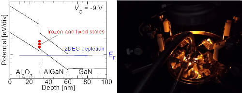
Energy band diagram of a next-generation compound semiconductor device (left) and measurement of
electronic properties (right)
Three-Dimensional Integrated Circuit (3D-IC) System Design Technology
Our research focuses on the design technology for LSI chip integration systems using three-dimensional stacking
with Through-Silicon-Vias (TSV) to achieve higher integration, increased chip-to-chip communication capacity and
speed, and reduced power consumption. Traditionally, semiconductor LSIs, along with other components, are placed
in a planar arrangement on printed circuit boards or interposers (silicon chips for wiring).
In our research, we target LSI chip integration systems based on three-dimensional stacking with TSVs. We aim to
develop design techniques that modularize and integrate various components within the target system, including
microprocessors, software, dedicated hardware (digital logic circuits), sensors, actuators, communication
modules, and power sources. This approach allows us to simulate and emulate the performance and power
consumption of the system during application operations before manufacturing, enabling thorough verification.
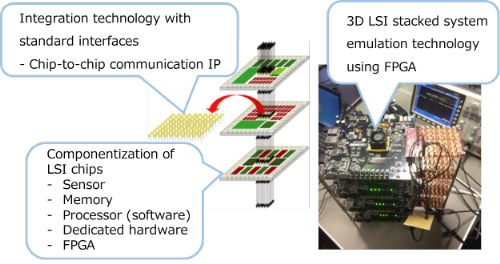
Three-Dimensional Stacked LSI System Design Technology: [Left] Concept of componentization of LSI chips
and system integration through chip-to-chip communication, [Right] Example of a Three-Dimensional
Stacked LSI System Emulator using FPGA.
